
High Thermal Conductivity PCB Solutions from Prototype to Low-Volume Production
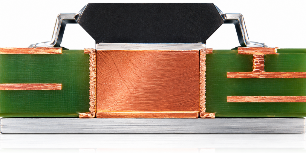
A Copper Coin PCB(also known as a Copper Inlay PCB) is an advanced thermal management solution that efficiently transfers heat away from high-power components through the shortest possible thermal path while maintaining excellent design flexibility.
As power devices and high-density electronic assemblies continue to generate more heat, effective thermal management has become essential for ensuring product performance, reliability, and long-term durability.
Customer Challenges / Request
The customer was experiencing excessive temperature rise on the PCB due to the mounting of high-power components. Their requirements include:
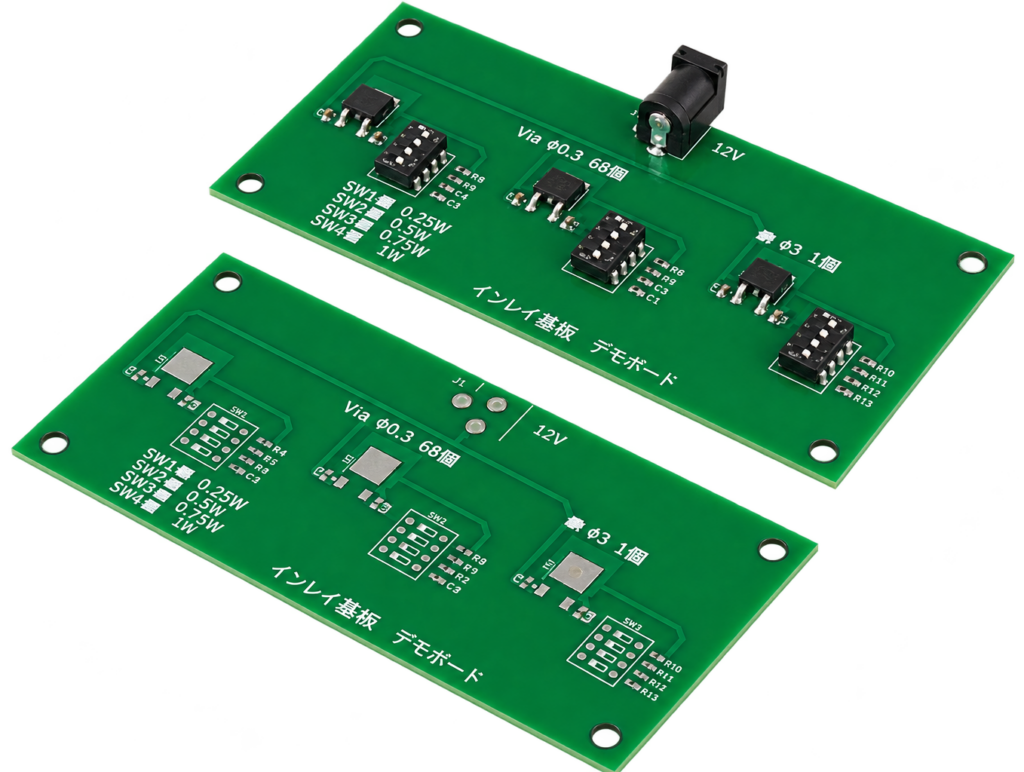
- Reduce the temperature rise around heat-generating components.
- Improve heat dissipation beyond what could be achieved with thermal vias alone.
- Avoid increasing the overall product size by adding heat sinks or other thermal management components.
- Support low-volume prototyping, which can be difficult for conventional mass-production PCB manufacturers.
During the prototyping stage in particular, many PCB manufacturers require dedicated tooling and minimum order quantities because their manufacturing processes are optimized for mass production. As a result, producing a single prototype board or accommodating design changes can be difficult.
Our Solution
After reviewing the requirements, Seiken proposed the following PCB structure:
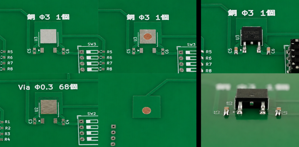
- Place a copper inlay directly beneath the heat-generating component.
- Add a dedicated thermal dissipation structure while maintaining the existing circuit design.
- Maintain the existing multilayer PCB structure.
- Optimize the design without sacrificing available component mounting area.
- Provide prototype production starting from a single board.
Results & Benefits
| 1. | Improved heat dissipation and reduced total cost: By incorporating a copper coin structure into the PCB, the following benefits can be achieved. |
| 2. | Improved heat dissipation: The copper inlay efficiently transfers heat away from heat-generating components, helping to suppress increases in component temperature. |
| 3. | Improved reliability: Copper has a lower coefficient of thermal expansion than aluminum. This can reduce stress on solder joints and contribute to improved long-term reliability. |
| 4. | Reduced assembly work: By integrating the heat dissipation structure into the PCB, separately installed heat dissipation components and mounting screws can potentially be eliminated, reducing assembly time and labor. |
| 5. | Reduced system cost: Reducing the number of components and assembly processes can help optimize the overall system cost. |
| 6. | Flexible support for prototypes and small-lot production: Because prototype production is available from a single board, customers can evaluate designs with lower risk during the early stages of development. |
Unlike conventional PCB manufacturers that primarily focus on mass production, Seiken can support small-lot prototypes, including production from just one board. We also provide technical consultation from the design stage. No initial setup fees or tooling costs are required, allowing us to respond flexibly to early-stage evaluations and design or specification changes.
Copper Inlay vs. Thermal Via: Performance Comparison
| PCB Thickness | Copper Inlay Diameter | Thermal Resistance of Copper Inlay | Thermal Vias Required for Equivalent Performance | Approx. Minimum Area Required for Via Array |
|---|---|---|---|---|
| 1.0 mm (Thin, high-thermal-performance) | φ2.0 mm | 0.82°C/W approx. | 145 vias | 4.8 × 4.8 mm² approx. |
| 1.0 mm (Thin, high-thermal-performance) | φ3.0 mm | 0.36°C/W approx. | 327 vias | 7.2 × 7.2 mm² approx. |
| 1.6 mm (Standard rigid PCB) | φ2.0 mm | 1.30°C/W approx. | 145 vias | 4.8 × 4.8 mm² approx. |
| 1.6 mm (Standard rigid PCB) | φ3.0 mm | 0.58°C/W approx. | 327 vias | 2.7 × 7.2 mm² approx. |
Thermal via conditions: Via diameter: φ0.3 mm; hole-wall plating thickness: 25 μm (typical specifications).
Note: The thermal resistance values are theoretical values calculated based on the bulk thermal conductivity of pure copper (390 W/m·K). Contact thermal resistance is not included.
Application
Copper inlay PCBs are particularly suitable for products that generate significant heat or require high reliability, including:
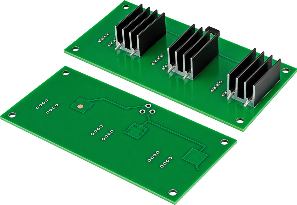
- Power semiconductor modules
- Power supply circuits and DC-DC converters
- Motor driver circuits
- Automotive electronics
- High-density PCBs
They are also suitable for pre-production evaluation, as well as PCBs with special layouts or unconventional shapes that can be difficult for conventional PCB manufacturers to accommodate.
Let’s Discuss Your Challenges
As electronic devices become increasingly sophisticated, thermal management has become a critical design consideration that directly affects product performance and reliability.
Copper inlay PCBs provide excellent heat dissipation and high reliability while maintaining design flexibility. They offer a high-performance thermal management solution that can be flexibly applied from prototyping through small-lot production.
If you are facing challenges such as:
- “Thermal management is becoming a problem.”
- “We want to prototype a high-thermal-performance PCB in a small quantity.”
- “Another PCB manufacturer was unable to support our requirements.”
Even for small-volume prototypes, Seiken can provide flexible PCB design and development without tooling costs, helping customers move forward with their evaluation and development projects. Please feel free to contact us for a consultation.