ProductsIntroduction of Testing Fixtures by Category

Semiconductors
We deliver tailored, high-precision solutions for every stage of semiconductor and PCB inspection—from early wafer-level testing to final quality checks post-packaging. Whether you’re dealing with fine-pitch layouts, high-current demands, non-magnetic environments, or high-frequency signals, our technologies are engineered to meet your specific testing challenges with accuracy and efficiency.
Front-End Process
Back-End Process
Wafer-Level Testing
Final Package Testing
Manufacturing
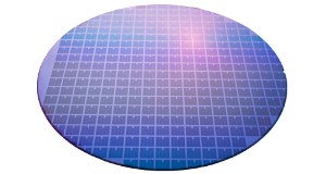
(bare dies)
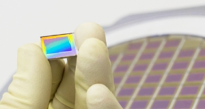

Testing
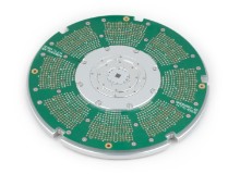
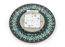
Advanced Probe Cards
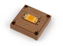
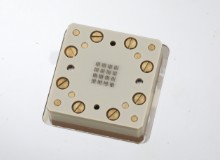
IC socket evaluation
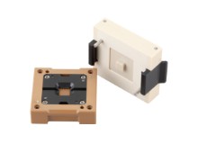
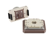
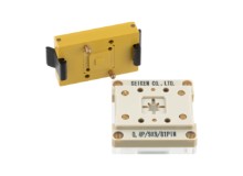
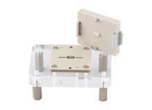
Probe Technologies
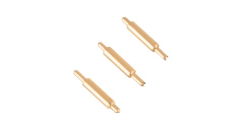
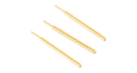
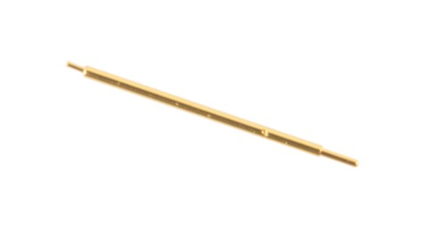
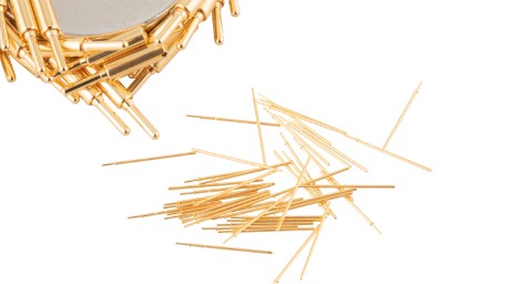
Printed Circuit Boards (PCB)
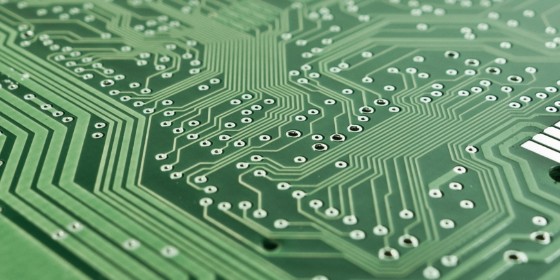
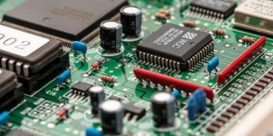
We support printed circuit board (PCB) inspection—both at the bare board stage and after component assembly.
Items subject to inspection
Inspection Fixtures
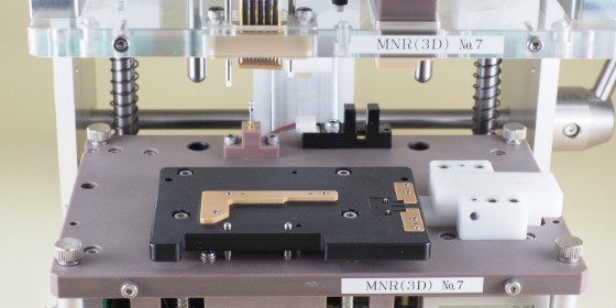
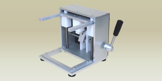
Type 1 (example)
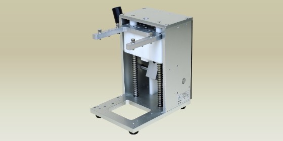
Type 2 (example)
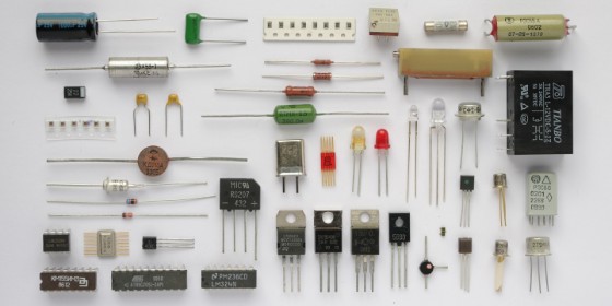
Electronic Components
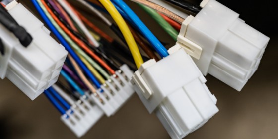
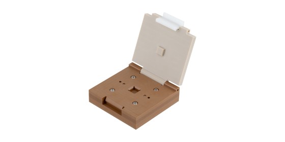
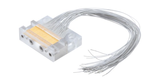
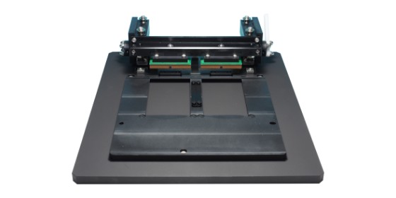
We support a wide range of inspections using test fixtures equipped with contact probes and specialized terminals. Whether your requirements involve fine-pitch components, high-current applications, non-magnetic materials, high-frequency measurements, among others, we offer optimal solutions customized to your specific testing environment.
Items subject to inspection
Inspection Fixtures
Others
From semiconductors and electronic components to automotive, aerospace, medical, telecom, energy, and robotics—Seiken’s contact probes and inspection fixtures are trusted across a wide range of industries.
Whether you’re in R&D, mass production, or custom product development, our flexible approach and deep expertise allow us to turn your ideas into test-ready realities. We also support related applications, including connector testing and early-stage product development.
Facing a complex inspection or connection challenge? Let’s solve it—together. We deliver precision and drive innovation.
