ProductsFine-Pitch Technology

Innovative Solutions for Advanced Test Environments
In semiconductor testing, cantilever probes are typically used for wafer-level inspection, while IC socket methods using double-ended probes are common packaging testing. However, as chip mounting technology evolves, more devices now feature fine-pitch bumps or copper pillars directly on the chip, making traditional cantilever methods less effective. The extremely tight, grid-like bump layouts make it difficult to position probe tips accurately.
At the same time, the demand for simultaneous multi-device testing with uniform and fine-pitch contact is increasing. This has led to the growing use of vertical probe cards and other high-density testing solutions. Seiken addresses these challenges by offering fine-pitch probes tailored to your pitch requirements, along with customized fixtures and board designs, delivering a total solution for advanced test needs.


Key Features & Advantages
01 Flexible solutions for diverse test environments
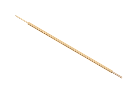
Seiken’s fine-pitch probes support pitches as small as 130µm. Combined with vertical probe cards, IC sockets, and other test fixtures, they ensure reliable contact with tightly arranged micro bumps, adapting to a wide range of testing environments.
02 Stable contact with micro bumps
We use special alloys with excellent solder affinity for the probe tip and support custom tip shapes such as crown cuts. This ensures stable and reliable contact, even with small bumps.
03 Enhanced connectivity powered our unique spring mechanism
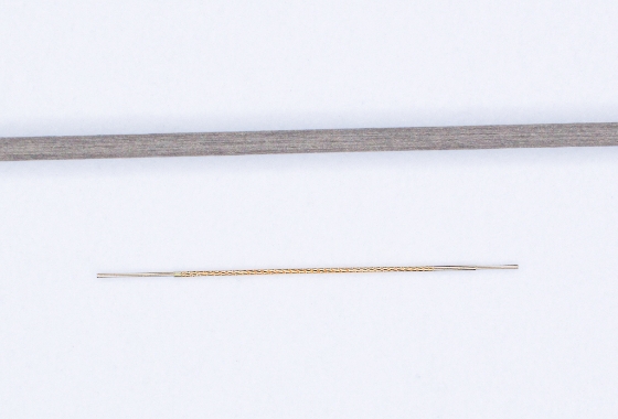
Seiken’s unique spring structure delivers consistent contact force and outperforms conventional single-pitch probe springs. This enhances contact reliability and boosts test accuracy, even under demanding conditions.
Application Examples
Explore more
- Wafer-level testing
- FPD (Flat Panel Display) inspection
- Electronic component testing
