ProductsAdvanced Probe Cards

High-Precision Solutions for Efficient Wafer Testing
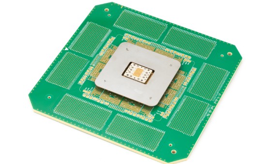
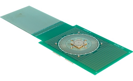
Our advanced probe cards are essential tools for wafer-level testing in semiconductor manufacturing. These cards enable accurate testing of IC chips before they are mounted onto substrates, helping to detect defects early in the production process and improve overall product quality. By transmitting and receiving electrical signals to each pin on the wafer, probe cards gather vital test data—ensuring each chip performs as expected. They play a critical role in identifying issues during the initial stages of semiconductor production.
Boost Testing Efficiency with Advanced Vertical-Type Probe Cards: Unlike traditional cantilever-type probe cards, our advanced vertical-type design supports simultaneous multi-die testing and full-wafer measurements. This dramatically increases throughput and reduces testing time.
Thanks to precision contact technology, these cards also support high-frequency and high-current testing with exceptional reliability. Their user-friendly design makes maintenance easy, minimizing downtime and maximizing productivity. Whether you’re aiming to streamline your testing process or improve measurement accuracy, we offer flexible solutions tailored to your requirements.
The Structure of Advanced Probe Cards
Seiken’s advanced probe cards are engineered for excellence, featuring a probe head and a probe card substrate (PCB). Every probe head is designed and manufactured in-house, utilizing high-precision machining technology. This approach guarantees accuracy, and performance you can trust.
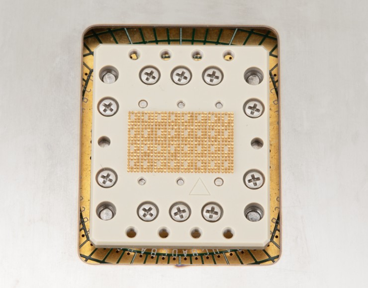
Probe head
Our probe heads are machined from engineering plastics or ceramics, shaped to fit your testing needs.
Available materials include
- Resin – plastics: Sumika Super, Topfine and other Engineering plastics.
- Ceramics: Photoveel, among others.
These materials provide excellent durability and stable probe fixation, helping to create the ideal testing environment.
Probe card substrates
We offer two PCBs types to suit your testing environment.
- Custom PCB (for mass production and performance-critical tests)
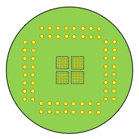
Designed specifically for each customer’s application, these PCBs allow for maximum customization and precise test conditions.
- General PCB
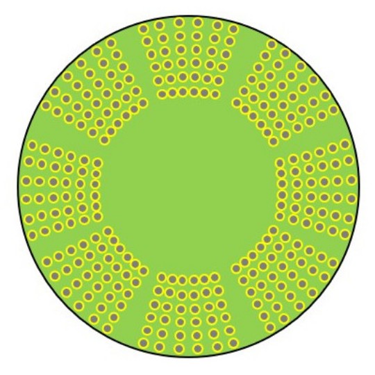
Compatible with many major tester manufacturers, these PCBs offer flexible setups using jumper wires and pin blocks to suit a wide range of tests.
Note: Some general PCBs are proprietary designs by Seiken—feel free to contact us for details.
Connection options: tailored to your testing needs
At Seiken, we offer versatile connection solutions to match your specific application.
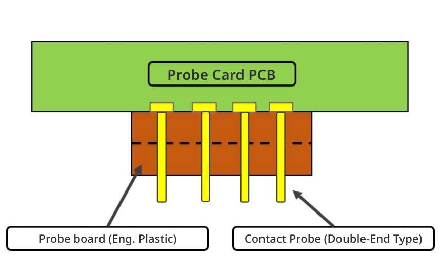
- Custom PCB (High precision, No wiring)
-
- Our direct-docking design connects the probe head to the PCB, eliminating internal wiring and minimizing signal loss.
- Advantages: Lower long-term costs for mass production environments.
- Ideal for: Applications with fixed device layouts.
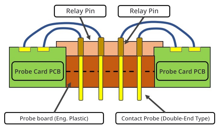
- General PCB (Flexible and Highly Compatible)
-
- Designed with a central opening, this configuration allows for flexible probe head mounting.
- Advantages: Excellent versatility for evolving designs.
- Considerations: Slightly higher wiring resistance, making it less suited for high-frequency or low-current testing.
Key Features & Advantages
01 Precise positioning and accurate measurement of individual chips
Our probe cards are engineered for versatility, easily flipping to enable individual chip testing after dicing. Optional guide frames and contact covers simplify chip alignment and ensure precise probing.
02 Easy maintenance with replaceable probes
Maintain peak performance with minimal downtime—our design allows the probe section to be replaced independently, eliminating the need to disassemble the entire fixture. This approach saves both time and maintenance costs.
03 Customized solutions, from single units to full production
At Seiken, we collaborate closely with customers to create probe cards tailored to their unique testing conditions and development requirements. Whether you need a one-off prototype or full-scale production support, we’re committed to delivering solutions that fit your needs at every stage.
Application Examples
Explore more
- Wafer-level testing
- IC design verification
- Debugging, etc.
