~The Crucial Role of Contact Probes~
What Is a Silicon Wafer?
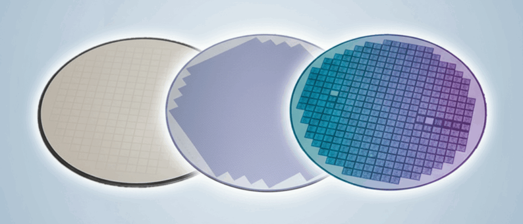
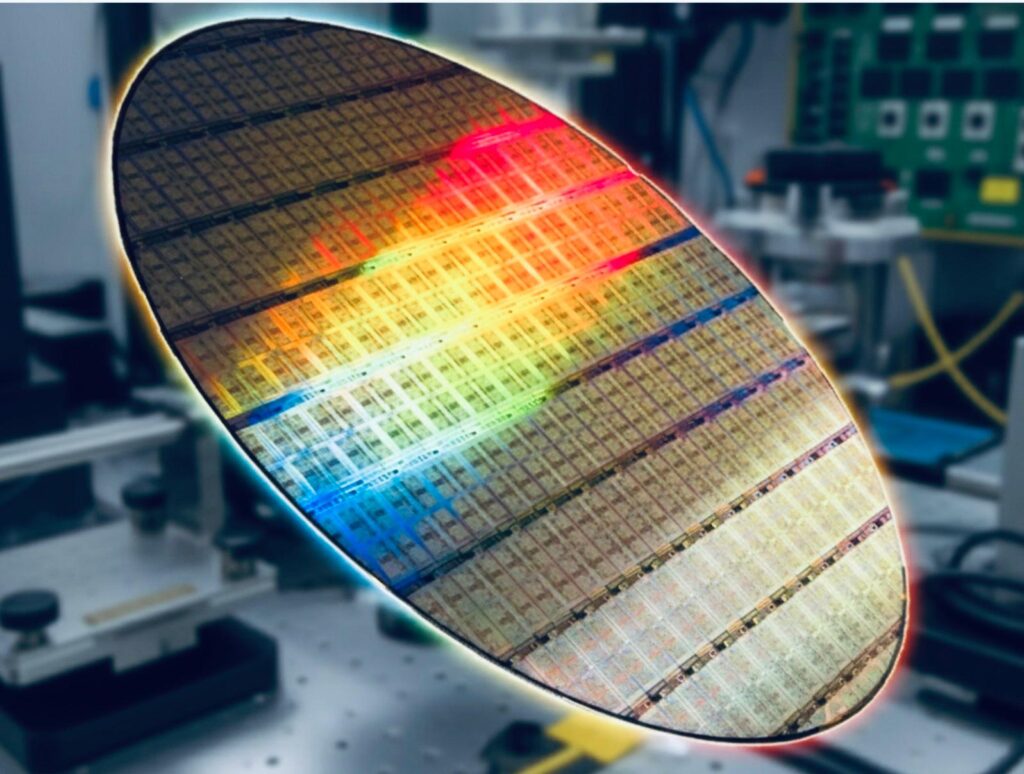
A silicon wafer (also known as slice or substrate) is the foundation of nearly every semiconductor device. It is a circular, mirror-like plate sliced from a high-purity single-crystal silicon ingot, then polished to extreme smoothness. Wafer diameters typically range from a few inches up to 300 mm. On each wafer, identical circuit patterns called dies are formed in large arrays through photo-lithography and other semiconductor processes. Later, these dies are separated and packaged into the chips that power everything from smartphones to satellites.
Basic terminology:
- Wafer: A circular substrate with multiple integrated circuits patterned on it.
- Die: A single chip after separation from the wafer.
What Is “Wafer Testing”?
Wafer testing is the process of electrically inspecting the chips before they are cut from the wafer. This step identifies defective circuits in advance, preventing unnecessary cost and time wasted on packaging non-functional chips.
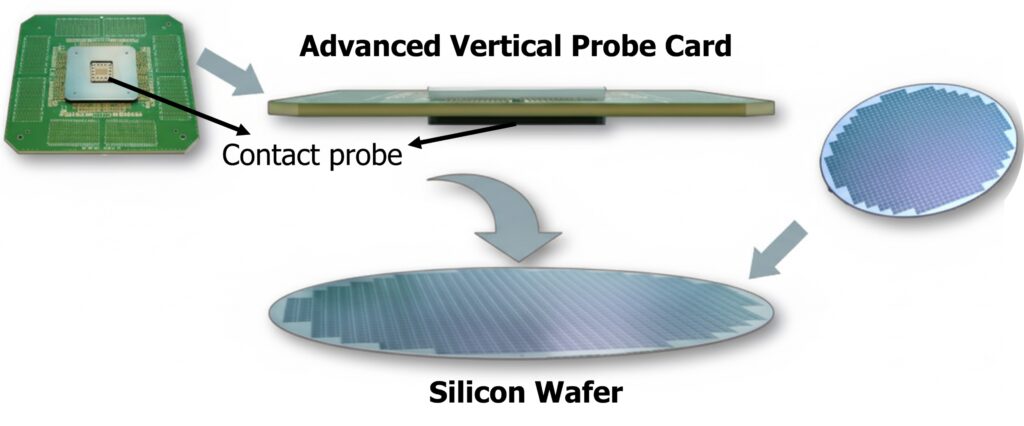
Testing is carried out using a probe card connected to a test equipment. The probes make contact with the wafer’s pads to send and receive signals.
Typical wafer-level inspections include:
- Continuity (open/short) testing
- Basic power-on functional checks (smoke tests)
- Memory read/write verification and analog IC measurements
- RF or high-current testing with specialized probe cards
Each application demands unique requirements for accuracy, speed, and probe contact performance.
Relationship Between Test Equipment and Probes
| Equipment / Component | Role |
|---|---|
| Wafer Prober | Holds and aligns the wafer precisely with the probe card — the stage for testing. |
| Probe Card | Interface that consolidates many probes. Types include cantilever and vertical, chosen based on application. Variants exist for RF, high-current, or non-magnetic use. |
| Contact Probe | Spring-loaded pins that deliver consistent force and high durability during repeated testing cycles. |
Key considerations:
- Signal integrity: In RF applications, probe impedance and ground layout must be carefully designed.
- Durability: Probes often endure millions of contact cycles in mass production.
with probe cards follows the same basic principle.
Seiken’s Strength — High-Reliability Probes × Engineering Capability
At Seiken, we integrate both probe manufacturing and probe card design, ensuring robust performance for every application.
- Proven expertise in high-current, RF, and non-magnetic probes.
- Prototyping available from just a single probe card.
- Custom probe card layouts tailored to your specific test requirements
Whether your process involves wafer-level testing, IC socket evaluation, or PCB-level inspection, Seiken delivers reliable contact solutions that safeguard measurement accuracy and product quality.
Discover how Seiken’s expertise can support your testing needs—contact us today to learn more.