Why Test Fixtures and Probes Are Essential Before Packaging
What Is a Bare Die (Die)?
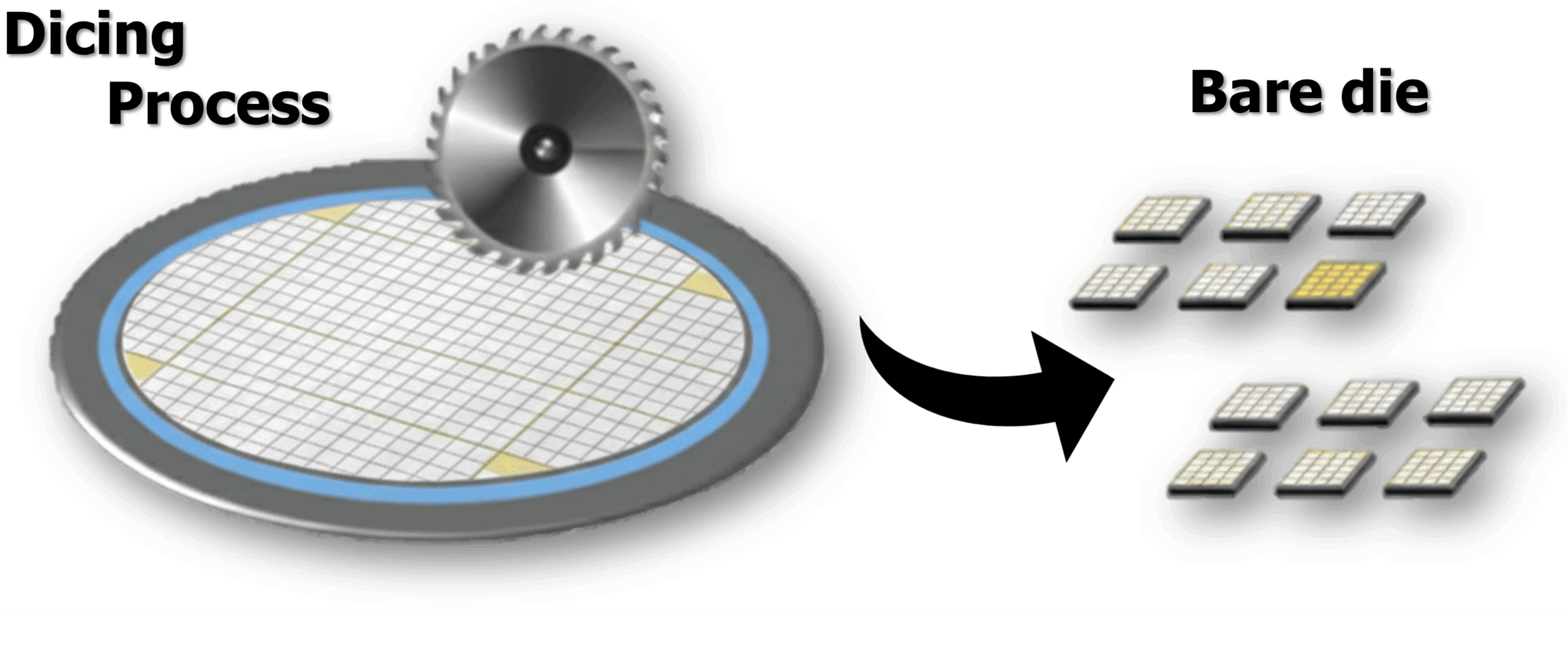
A die is the smallest functional semiconductor unit created on a wafer. After the wafer is cut (diced), each circuit becomes an individual die. When the chip remains unpackaged, it is referred to as a bare die.
Testing at the die level is critical to verify electrical characteristics, ensure long-term reliability, and screen out defective chips before costly packaging steps.


Common Measurements at the Die Level
Die Probing:
The die is mounted on a chuck, and test probes make direct contact for electrical inspection.
Die Sorting:
Good dies are separated from defective ones before assembly. This is particularly important for multi-chip modules and high-value devices, where one faulty die could compromise the entire product.
Fixtures and Contact Probes for Die Testing
| Equipment / Fixture | Role |
|---|---|
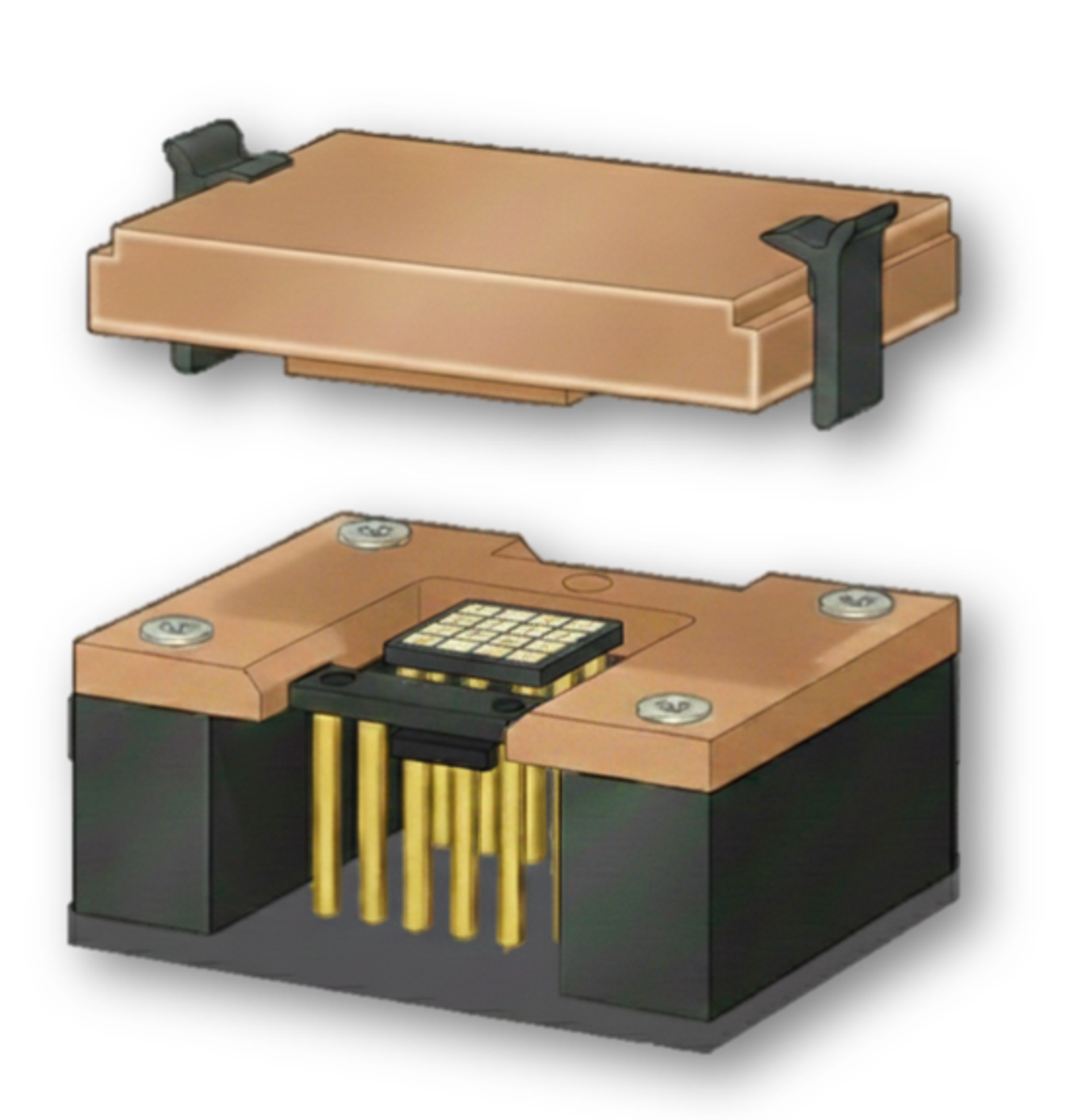
| Die Handler | Transfers bare dies and holds them for electrical inspection. Internal sockets often integrate spring probes. |
| Die Prober / Micro Prober | Precisely aligns fine-pitch pads on small dies for accurate electrical contact. |
| IC Test Socket | Provides temporary connection for bare dies or small packages. Spring probes allow repeated insertion, making it ideal for mass evaluation. |
Across all these tools, spring contact probes remain the critical interface for stable, repeatable measurements.

Technical Challenges in Die Testing
- Microscale precision: Pads can have small pitches, leaving no room for probe misalignment.
- Stress and heat management: Excessive force or thermal effects can damage the die.
- Contact resistance stability: Even tiny inconsistencies at probe tips may lead to false test results.
Seiken’s Solution — Precision Fixtures with Advanced Probing Technology
Seiken combines probe design with fixture engineering to deliver complete testing solutions:
- Probes supporting narrow pitches down to 130 µm
- Custom specifications for ultra-low force, high current, or high temperature applications
- Optimal pin layout and probe force design for each customer’s testing scenario
In die testing, where both positional accuracy and contact stability are indispensable, Seiken’s Spring probe expertise ensures reliable results and improved yield across diverse semiconductor applications. Please feel free to contact us if you have any special requests.
