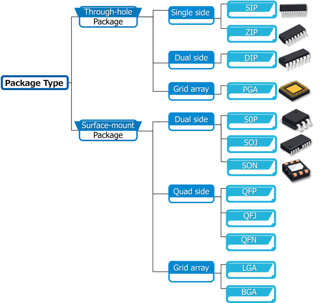
~SOP, SOJ, and SON? A Simple Comparison of Major Semiconductor Package types~
SOP, SOJ, and SON are representative surface-mount semiconductor packages that have supported electronic device miniaturization from the early days of surface-mount technology (SMT) to the present. Unlike through-hole packages, surface-mount packages are soldered directly onto the surface of a printed circuit board (PCB), enabling higher mounting density and thinner product designs.
Key Characteristics of Surface-Mount Technology
- Terminals or leads are soldered directly to the PCB surface
- High mounting density and space efficiency
- Ideal for thin, lightweight, and compact devices
- Highly compatible with automated SMT assembly for mass production
Today, surface-mount packages are the global standard in electronic manufacturing. From smartphones and notebook PCs to automotive ECUs and industrial control systems, most modern circuit boards are dominated by surface-mount components.
Below, we introduce three widely used package types along with their structural features and inspection requirements.
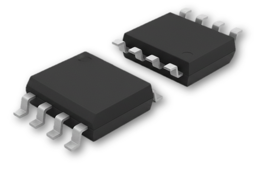
SOP (Small Outline Package)
The Standard Package for Surface-Mount ICs. SOP is a surface-mount adaptation of the DIP package, featuring a thinner body and finer lead pitch. Its most recognizable feature is the gull-wing–shaped leads extending from both sides of the package. Its key features include:
- Lower profile and smaller footprint compared to DIP
- Suitable for automated reflow soldering
- Available in multiple variations: TSOP (Thin SOP), SSOP (Shrink SOP), MSOP (Mini SOP)
SOP packages are widely used in, notebook PC peripheral modules, control ICs for consumer electronics, sensors and small driver ICs, EEPROMs, ADCs, and more.
Thanks to their excellent cost performance, mature manufacturing process, and wide availability, SOP packages remain a mainstay for general-purpose ICs.
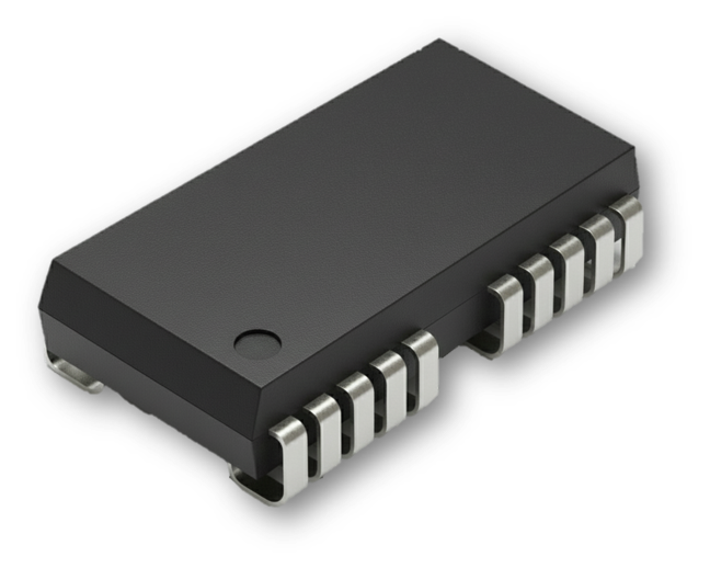
SOJ (Small Outline J-Leaded)
The J-Lead Package That Supported Early Memory Devices. SOJ packages resemble SOP in outline but differ in lead shape. Their J-shaped leads are bent inward and wrap underneath the package, providing enhanced mechanical retention. Its key features include:
- Strong solder joints due to J-lead structure
- Reduced risk of lead deformation
- Historically adopted as a standard package for memory devices
SOJ packages are used in DRAM (from 256K to early SDRAM generations), SRAM,
certain communication and control ICs, among other applications.
While SOJ has largely been replaced by BGA packages in new designs, it is still used for maintenance, repair, and replacement in legacy systems.
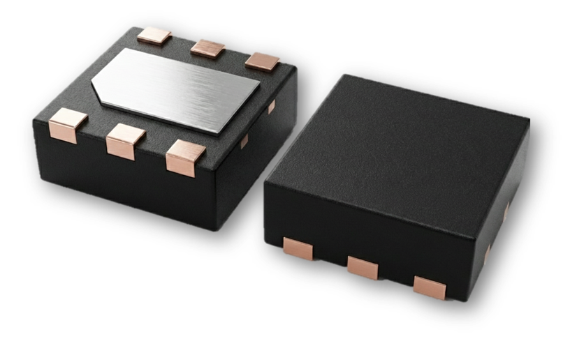
SON (Small Outline Non-Leaded)
Compact, Lead-Less Packages for High-Performance Electronics. SON is a lead-less surface-mount package that uses metal pads on the bottom of the package instead of external leads. By eliminating protruding leads, SON significantly reduces parasitic inductance and electrical noise.
Often regarded as a compact, two-sided version of QFN, SON packages offer excellent electrical and thermal performance. Its key features include:
- Lead-less and extremely thin profile
- Low inductance, ideal for high-speed and high-frequency applications
- Cost-effective for high-volume production
- Many types include exposed thermal pads for efficient heat dissipation
They are mostly used in smartphones and mobile devices, RF and wireless communication ICs, power ICs (regulators, charger ICs), sensor ICs and more.
SON has become an essential next-generation surface-mount package for modern, high-density electronic designs.
Technical pros and cons of SOP, SOJ, and SON
| Advantages | Disadvantages |
|---|---|
| SOP ・Gull-wing leads allow easy soldering and automated assembly ・Good visual inspection and reworkability ・Wide variety of pin counts and sizes, highly versatile for general-purpose ICs | SOP ・Thicker package compared to leadless types ・Higher parasitic inductance, less suitable for high-frequency applications ・Larger footprint on the PCB |
| SOJ ・J-lead structure provides high mechanical strength ・Less prone to lead damage or deformation ・Proven reliability, especially in memory applications (e.g. DRAM) | SOJ ・Solder joints are difficult to visually inspect ・Rework is more challenging ・Usage is declining in modern designs |
| SON ・Leadless structure enables very thin, compact packages ・Low parasitic inductance, well suited for high-frequency applications ・Excellent thermal performance when using exposed thermal pads ・Supports high-density PCB layouts | SON ・Assembly process requires precise PCB and solder control ・Visual inspection and rework are difficult ・PCB design complexity and initial design cost are higher |
Fixtures required in SOP, SOJ, and SON inspection and test processes
For SOP, SOJ, and SON packages, fine lead pitch, compact size, and limited contact areas present significant inspection and testing challenges. High-precision IC sockets and contact probes are essential to ensure stable electrical contact.
Common Inspection Challenges
- Fine lead pitch, often 0.4 mm or less
- Very small contact areas on lead-less SON terminals
- High durability requirements for fixtures used in automated test systems
Seiken’s Solutions for Through-Hole Package Testing
| Challenge | Example solutions from Seiken *Click on each solution to learn more. |
|---|---|
| Reliable contact on fine-pitch SOP leads | Fine-pitch probes |
| Stable load on curved SOJ J-leads | Custom probe stroke and load designs |
| Damage-free contact with SON pads | Customized probe tip geometries |
Seiken provides one-stop support, from probe selection to fixture design and manufacturing, supporting applications ranging from mass-production testing to evaluation and reliability testing.
Standard Packages for Today—and Tomorrow
As electronic devices continue to become smaller, thinner, and more power-dense, surface-mount packages such as SOP, SOJ, and SON will continue to evolve. In parallel, inspection technologies must advance to meet demands for finer pitch, higher precision, and greater reliability.
If you are facing challenges in IC inspection or testing, please feel free to contact us. Our engineers will be pleased to propose the optimal probe and fixture solutions for your test environment.