From QFP to BGA and WLP: A Complete Overview of Semiconductor Packages
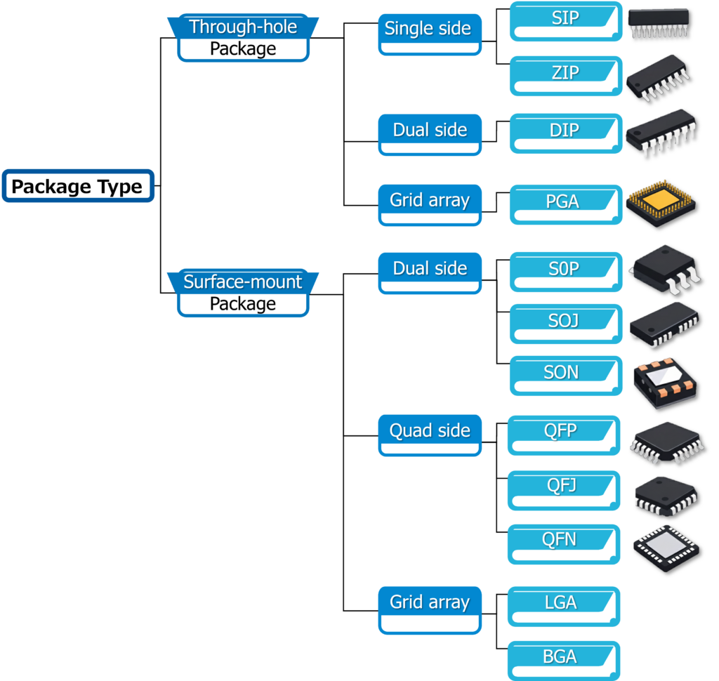
QFP, QFJ, & QFN are some semiconductor packages, and semiconductor packages are broadly classified into through-hole packages and surface-mount packages. Through-hole packages insert leads into PCB holes and solder them on the reverse side. In contrast, surface-mount packages solder leads or electrode pads directly onto the PCB surface, offering superior thinness, light weight, and high mounting density.
The Evolution of four-sided Lead Packages for High Pin Counts
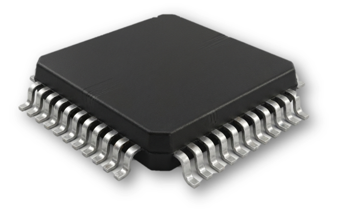
QFP (Quad Flat Package) — High-I/O Packages with Leads on All Four Sides
QFP places gull-wing leads on all four sides of the package, enabling very high pin counts. It has many variants, such as TQFP (Thin), LQFP (Low-profile), and fine-pitch versions with reduced lead spacing. QFP key features are:
- Supports hundreds of pins
- High signal density, suitable for complex LSIs
- Easy to inspect, replace, and rework despite being surface-mount
- Moderate thermal performance compared to newer package types
The QFP is widely used in microcontrollers, ASICs, motor control ICs, and audio and image processing devices.
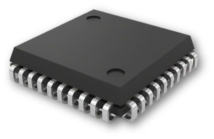
QFJ (Quad Flat J-leaded) — High-Reliability Packages with J-Leads
Like QFP, QFJ has leads on all four sides, but uses J-shaped leads that curve inward under the package. This type of package is commonly known as PLCC (Plastic Leaded Chip Carrier). Compared with QFP, QFJ offers a more compact footprint and improved mechanical strength. QFJ key features include:
- High mechanical strength due to J-leads
- Excellent vibration resistance
- Higher mounting density than DIP and greater robustness than QFP
QFJ may be found in industrial ICs, memory and communication ICs, and specialized control ICs.
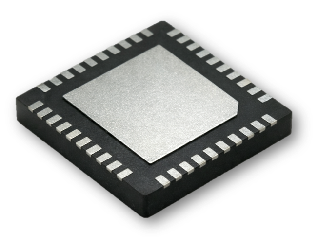
QFN (Quad Flat No-leads) — Today’s Mainstream Lead-less Package
“Flat” and “leadless,” QFN places electrode pads around the perimeter of the bottom surface and eliminates external leads. QFN key features are:
- Ultra-low profile (many packages are under 1 mm thick)
- Excellent electrical performance (low parasitic inductance and capacitance)
- High thermal performance via a central exposed thermal pad
QFN is widely used in power ICs (PMICs, DC-DC converters), RF ICs (Bluetooth, Wi-Fi), sensor ICs, and analog ICs. QFN is now one of the most widely used surface-mount packages, widely adopted in modern compact, high-speed devices including 5G and power-management applications.
Technical pros and cons of QFP, QFJ, & QFN
| Advantages | Disadvantages |
|---|---|
| QFP • Easy to assemble and visually inspect, even for high pin-count devices (100–300+ pins) • Gull-wing leads make solder joints clearly visible for inspection • External leads allow relatively easy rework and repair • Mature manufacturing process ensures stable mass production and good yields • Suitable for hand soldering, making it ideal for prototyping and development | • Larger PCB footprint due to outward-extending leads • Longer leads increase parasitic inductance and capacitance • Less suitable for high-speed or RF applications • Limited thermal performance (not ideal for high-power ICs) • Fine-pitch versions increase the risk of solder bridging |
| QFJ • J-lead structure enables a more compact package size • Inward-curving leads are less prone to damage during handling and assembly • Leads help absorb mechanical stress, improving reliability • Compatible with socket mounting | • Solder joints are harder to see, making visual inspection difficult • Rework is more difficult compared to QFP • Limited scalability to very high pin counts • Increasingly being replaced by QFN and BGA, leading to reduced adoption |
| QFN • Leadless design enables compact size and high-density mounting • Short connections reduce parasitic inductance, making it ideal for high-speed signals • Excellent thermal performance thanks to the exposed thermal pad • Can be up to ~40% smaller than QFP for the same pin count • Well-suited for compact electronics such as mobile and IoT devices | • Often requires X-ray inspection to detect soldering defects • Rework is more difficult • Solder joint reliability must be carefully designed for thermal cycling environments |
Fixtures required in QFP, QFJ, & QFN inspection and test processes
Testing methods differ depending on the package shape. QFN presents particular difficulty because the soldered terminals are not visible. Typical challenges include:
- Lead pitch shrinking to 0.3 mm or less
- Extremely small pad areas on QFN
- High difficulty of measuring high-frequency and high-speed signals
- Precise load control required for multi-pin contact
- Special probe tips for J-lead shapes
- Alignment fixtures for accurate positioning
- Fixtures compatible with temperature testing
Seiken’s Solutions for QFP, QFJ, & QFN Package Testing
| Challenge | Example solutions from Seiken *Click on each solution to learn more. |
|---|---|
| Misalignment with fine-pitch leads | High-precision hole machining ensures near-theoretical pin positioning; guide frames are lot-adjusted to maintain alignment. |
| High-Current Testing Requirements | Our HC-C solution enables stable, reliable performance under high-current conditions. |
| Temperature testing | Heat-resistant probes |
Seiken provides advanced technologies optimized for high-pin-count and fine-pitch QFP and QFN packages. For thermal pad contact, special wide-area surface probes are used to ensure stable electrical and thermal contact.
High-Performance Packages for the Surface-Mount Era
QFP, QFJ, & QFN represent the evolution toward higher pin counts and higher speeds in surface-mount technology. Their testing requires high-precision fine-pitch contact, temperature compatibility, and accurate load control—all supported by Seiken’s probe and fixture technologies.
If you have any challenges with package testing, feel free to contact us.
We will be happy to propose the most suitable test solution for your application.