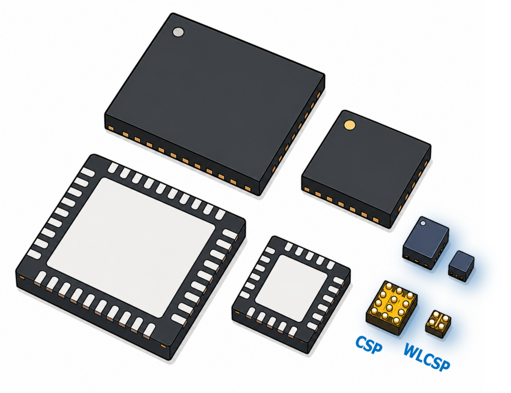
Discover why CSP & WLCSP are essential for high-density semiconductor devices
CSP & WLCSP are becoming essential semiconductor packaging technologies as electronic devices continue to evolve toward smaller sizes, higher speeds, and greater performance. These advanced chip-scale packages enable high-density mounting, improved electrical characteristics, lower power consumption, and greater design flexibility within extremely limited spaces, making them critical for modern smartphones, wearable devices, automotive electronics, and high-performance semiconductor applications.
Widely used in smartphones, IoT products, automotive electronics, etc., CSP and WLCSP have become indispensable technologies for next-generation semiconductor applications. Their compact structure, however, also introduce new inspection and testing challenges that require highly advanced probing solutions.
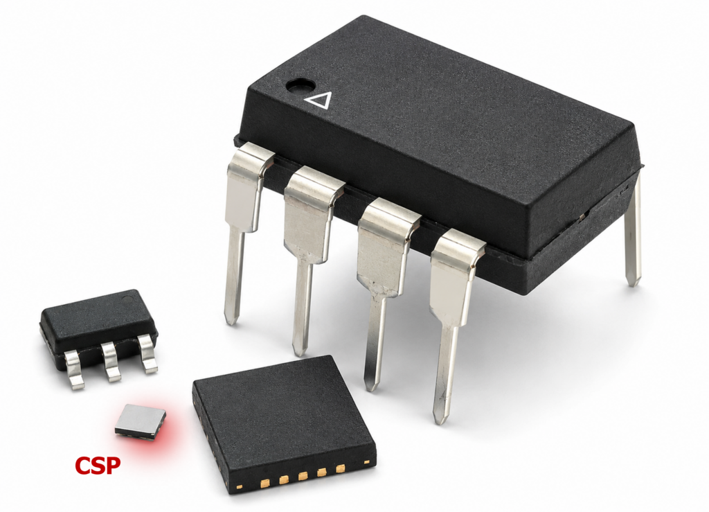
CSP & WLCSP: High-Density Chip-Scale Packaging
CSP (Chip Scale Package): Compact Size with High Reliability
CSP is a semiconductor package technology designed to keep the package size nearly identical to the die size itself. By minimizing package dimensions and shortening electrical pathways, CSP enables high-speed signal transmission, lower power consumption, and improved device miniaturization.
Because of its balance between compactness and reliability, CSP is widely adopted in mobile electronics, compact consumer devices, and high-performance semiconductor applications.
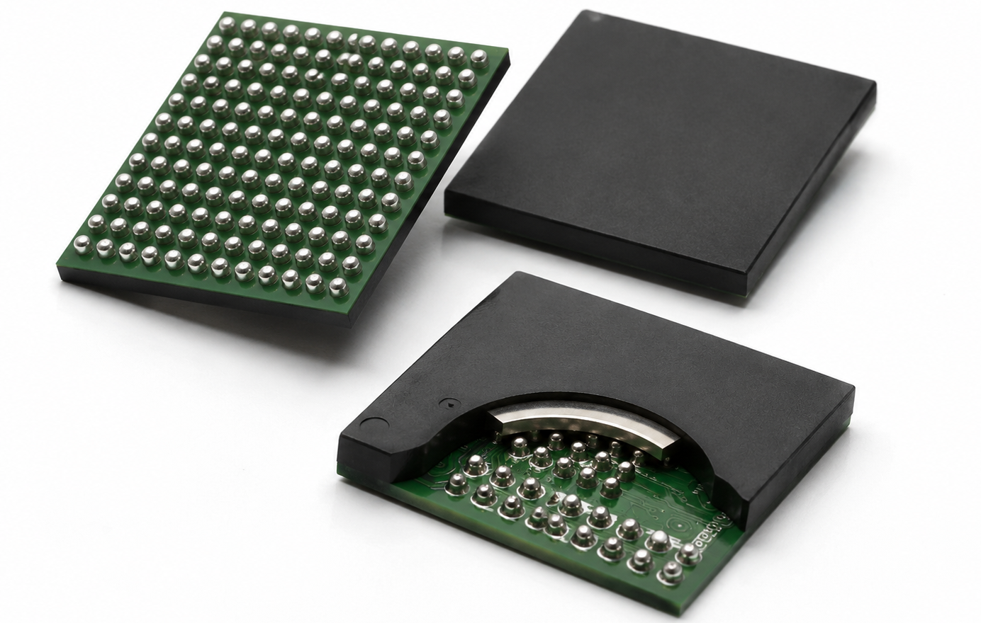
WLCSP (Wafer-Level Chip Scale Package): True Chip-Scale Integration
WLCSP takes miniaturization one step further by completing the packaging process directly at the wafer level before dicing. Redistribution layers (RDL) and bump formation are created on the wafer itself, allowing the final package size to remain nearly identical to the silicon die.
This advanced semiconductor packaging technology enables extremely thin form factors, excellent electrical characteristics, and high-density integration, making WLCSP one of the most widely used packaging methods for smartphones, RF devices, PMICs, and compact sensor modules.
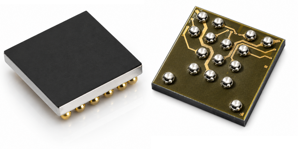
Key Features and Structure of CSP & WLCSP Packages
・Fine-Pitch Bump and Ball Configuration
CSP and WLCSP packages use micro solder balls, copper pillar bumps, or pad arrays on the underside of the package for board-level connections. As semiconductor devices continue evolving toward higher performance and greater I/O density, bump pitch has become increasingly smaller, with many advanced devices requiring pitches below 0.4 mm.
・Excellent Electrical and Thermal Performance
Because the interconnection is positioned very close to the semiconductor die, parasitic inductance and capacitance are minimized, resulting in superior high-frequency and high-speed signal performance. Thermal management also becomes increasingly important, requiring optimized substrate and PCB heat dissipation design.
・Wafer-Level Packaging Advantages
WLCSP technology simplifies backend processing by performing packaging directly on the wafer, reducing assembly complexity while enabling thinner and lighter semiconductor devices.
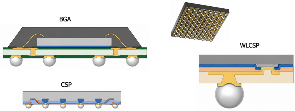
CSP and WLCSP are ideal semiconductor packaging solutions for compact, high-performance electronic products that require advanced miniaturization and high-density mounting. These technologies are widely used in smartphones, wearable devices, IoT equipment, RF front-end modules, PMICs, AI edge devices, automotive electronics, and compact sensor modules. In particular, WLCSP has become one of the leading advanced packaging technologies for modern mobile devices and high-frequency semiconductor applications due to its ultra-small size, excellent electrical performance, and ability to support highly integrated designs.
Difference between QFN, BGA, CSP, and WLCSP packages
| Package | Key Features | Typical Applications |
|---|---|---|
| QFN | Leadless package structure suitable for thin, low-cost designs with strong thermal performance. | Power ICs, analog ICs, automotive and industrial equipment. |
| BGA | Grid-array terminal structure supporting high pin counts and high-performance devices. | CPUs, GPUs, communication systems. |
| CSP | Near chip-size package optimized for high-speed, low-power, high-density designs. | Mobile and IoT devices. |
| WLCSP | Ultra-miniature wafer-level package offering superior miniaturization and electrical performance. | Smartphones, RF devices, wearable products. |
Inspection and Testing Challenges for CSP & WLCSP
As semiconductor packages continue shrinking, semiconductor inspection technologies must achieve significantly higher precision and durability.
・Narrow-Pitch Inspection Requirements
As semiconductor packages continue to shrink, CSP and WLCSP testing demands higher precision and more advanced contact technologies than ever before. Standard CSP devices typically feature bump pitches of 0.4–0.5 mm, while many WLCSP devices use ultra-fine pitches below 0.3 mm. These fine-pitch applications require highly accurate crown-cut probes capable of delivering stable, reliable contact without damaging delicate bumps.
・Multi DUT testing
In advanced wafer-level testing, WLCSP devices are often tested in multi-DUT configurations, where multiple DUTs are contacted simultaneously on the wafer. This creates the need for high-pin-count, high-precision probe cards engineered for exceptional alignment accuracy and electrical performance.
Seiken’s Solutions for CSP & WLCSP Inspection
We provide advanced testing solutions designed for high-current applications, non-magnetic environments, Kelvin measurements, and other demanding semiconductor test requirements. Whether you are developing next-generation CSP or WLCSP devices, our technologies help improve test reliability, measurement accuracy, and overall production efficiency.
| Challenge | Example solutions from Seiken *Click on each solution to learn more. |
|---|---|
| High-Precision Alignment | Support for narrow-pitch applications down to approximately 130 μm pitch, enabling simultaneous multi-bump inspection using vertical probe card technology. |
| Stable Contact Resistance | Flat and crown-tip probe designs allow stable electrical contact with minimal contact force, helping reduce bump damage during testing. |
| High-Temperature Durability | Heat-resistant probe materials and optimized spring structures support demanding high-temperature and high-current semiconductor testing environments. |
Seiken offers a wide range of contact probes, probe cards, and IC sockets optimized for advanced semiconductor package testing applications, including narrow-pitch CSP and WLCSP devices.
With extensive technical expertise and proven industry experience, Seiken helps customers solve inspection challenges related to semiconductor miniaturization, stable electrical contact, thermal durability, and high-density package testing.
If you are looking to improve probing stability, inspection precision, or narrow-pitch semiconductor testing performance, please feel free to contact us for technical consultation.