~An illustrated guide that makes semiconductor packages easy to understand at a glance~
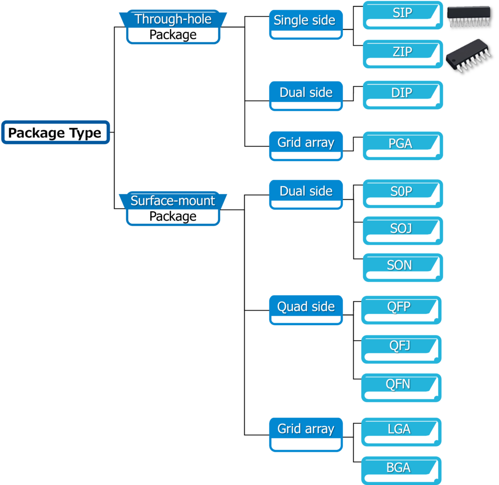
SIP and ZIP are semiconductor packages. Semiconductor packages are broadly classified into through-hole packages and surface-mount packages.
Through-hole packages insert pins into through-holes in a board and secure them by soldering. Compared with today’s surface-mount technologies, this is a more classical technique. Nevertheless, through-hole packages remain firmly used for:
- Applications requiring high mechanical strength
- Components that carry large currents
- Educational and experimental circuits (breadboard-compatible)
Historically important through-hole packages include SIP/ZIP (single-row), DIP (dual in-line), and PGA (grid array with many pins). Below we explain each of them and how they relate to fixtures and contact probes used in inspection and test processes.
SIP and ZIP — The origin of the mounting-density improvements pioneered by single-row packages
The birth of single-row packages
SIP and ZIP are through-hole packages that grew from the very simple idea of arranging pins in a single row. Before surface-mount technology existed, they played an important role in increasing circuit scale within limited board area.
・SIP: pins in a straight line ・ZIP: pins arranged in a zigzag pattern
Although structurally similar, they differ clearly in how they approached higher density.
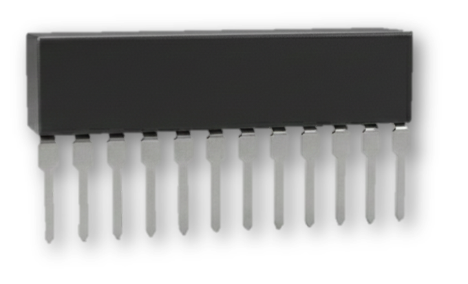
SIP (Single In-line Package)
SIP is a long, narrow package with leads arranged in a single vertical row on one side. Its characteristics include:
- Relatively high mounting density
- Intuitive layout and easy for prototyping
- Suited to designs that have allowance in the height (z) direction
Historically used for:
・Resistor arrays ・Sensor ICs ・Small analog modules
Today SIPs are less common in the general market, but they are still used in industrial applications that require elongated modules.
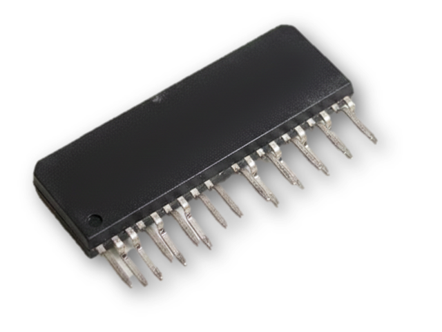
ZIP (Zigzag In-line Package)
ZIP is a higher-density improvement on SIP. ZIP shortens package length while effectively increasing neighboring pin spacing by bending pins into a zigzag arrangement.
When ZIP first appeared it was a key package to cope with rapidly increasing memory integration.By reducing the mounting area:
- Widely adopted for memory ICs, especially DRAM
- Can have a smaller footprint than DIP
- Able to meet demands for increased pin counts
Recently modern high-density packages like BGA have largely replaced ZIP, so ZIP today is limited to narrower uses such as analog ICs or some power modules.
Technical pros and cons of SIP and ZIP
| Advantages | Disadvantages |
|---|---|
| Simple structure, easy to manufacture | Requires height, so unsuitable for thin/low-profile designs |
| Leads are robust; high mechanical strength | Physical limits to high pin counts (SIP/ZIP have significant physical constraints) |
| Easy to repair/replace — ideal for education | Lower mounting density compared with surface-mount technologies |
Fixtures required in inspection and test processes
Inspection characteristics for SIP and ZIP
Because of their elongated shape and single-row pins, lead parallelism and contact stability strongly affect inspection accuracy. Therefore:
| ・SIP-dedicated IC sockets | ・Contact blocks using vertical probes |
| ・ZIP deep-insertion type sockets | ・Manual fixtures (with insertion guides) |
At Seiken, we can meet inspection requirements such as:
| Challenge | Example solutions from Seiken *Click on each solution to learn more. |
|---|---|
| Ensuring contact stability for long, narrow packages | Customized spring probes and fixtures |
| Multiple contact points on narrow-pitch ZIP | Fine-diameter, low-force probes |
| Integration into automated inspection lines | Probe blocks integrated with fixtures |
ZIP in particular can have cases where pin angles are slightly off; highly compliant spring probes are effective in following such variations.
SIP and ZIP are classical compared with today’s high-density packages, but they are historically important packages that supported the early stages of mounting-density improvements. There remains steady demand—especially in industrial applications—and their inspection often encounters contact issues caused by lead variability and narrow pitch.
If you are experiencing problems in your inspection process, such as unstable contacts or yield not improving with current fixtures, please feel free to contact us.
We can help you build an optimal inspection environment.